| This circuit is a follow up to the MOS Doubler (tm) that
I did a while back. I did this one to test the supposition that if you
generate a good octave by cancelling out everything except the
distortion in a circuit, then you could get back the signal mixed with
as much of the distortion as you liked by un-balancing the cancellation
circuit. Turns out that it works.
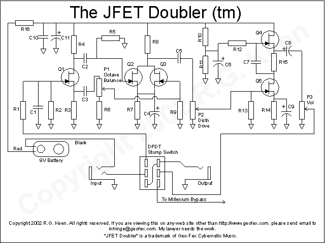
Here's the circuit. I revamped the phase inverter and output amp to suit an all-JFET circuit just for grins. The signal enters through R1, and any RF over 1MHz is shunted to ground by C1. R2 holds the gate of J1 at ground. The conduction of Q1's channel biases Q1 by raising the voltage on its source by the amount of current flowing through R3. I used 2N5485's, as I had these and the Vgsoff is about right. You can adapt this to many JFETs by changing the value of R3 to get the source voltage to between 1.5 and 3V, and then putting the same value in for R4 so it's still a phase splitter. In my circuit, R3 of 2.2K worked fine. The signals at the source and collector of Q1 are equal magnitude, but opposite phase, as befits a phase inverter.
The two phase-opposite signals are fed through C2, C3, R5, and R6/P1 to the opposing gates of the signal canceling pair, Q2 and Q3. For the best octave results, Q2 and Q3 should be matched. This is what led me to use the MOSFETs in a CD4007 in the MOS Doubler originally. GFR suggested JFETs, but getting matched MOSFETs (also a square-law device) for cheap in a CMOS IC was very attractive. Of course, the CMOS had its own problems. The additional isolation junctions and the connections to other devices internally in some CMOS modules made it tricky to get running. JFETs being isolated devices won't have either the connection problems - or the inherent matching. If you're up for matching, get them as close as you reasonably can with the JFET Matching Fixture. They needn't be perfect, but the better you do here, the more predictably it will operate. The signal canceling pair are biased by R7. I made R7 4.3K to get about 1.9V at the joined sources of Q2 and Q3. You may have to adjust this value to get a reasonable voltage across R8. I used 10K for R8, and it wound up with 3V across it. You have some leeway, but you should be prepared to tweak the values. P1 is called an octave balance control. When it's full up, the mirror imaged signals from Q1's source and collector drive the gates of Q2 and Q3 out of phase, so the the signal that appears on the joined drains is cancelled. If Q2 and Q3 were distortionless, there would be NO signal at their joined drains. However, Mother Nature being the lady she is, there are no distortionless devices, and so Q2 and Q3 both distort in their own way. It's a peculiarity of distortion that even order distortion is single directional; this means that Q2 and Q3 generate second order distortion that zigs the SAME way instead of opposite, so the second order distortion products reinforce at the drains instead of cancelling. The signal is rejected by the amount that the devices are matched, the distortion is reinforced and amplified, so what appears at the drains is largely second harmonic distortion and a smattering of other junk. But that only happens for perfect balance on the signal we feed in. If we deliberately unbalance the signal in, the cancellation of the base signal is not perfect. That's what P1 does. It lowers the signal from the source of the phase inverter by as much as half - P1 is a 50K pot, R6 is a 51K resistor. This allows us to unbalance the cancellation and get mostly signal with a little second harmonic. Since the signal is about 20db (10 times) as large as the distortion to start with, even a little imbalance puts a lot of signal on the drains. That's why you need to match Q2 and Q3 - if they're too far off, you can't get a good, solid octave. In either case, the signal and second harmonics appear at the drains of the canceling pair, and feed P1, the distortion drive pot. This is just a level control to feed a final amplifier. Since the distortion products can be quite small, we may need a lot of gain to bring them back up. I flipped in a SRPP-style gain stage. The inclusion of R15 (1K) ensures that the stage can drive reasonable loads out of it (see the article on JFET pairs and gain stages) instead of being loaded into low gain as a bare mu-amp can be (see the original National Semiconductor app note for more on the JFET mu-amp). This lets us make P3 the volume control be 100K, and still have a good chance of driving a low impedance load on the output. We would have to use yet another device as a follower to buffer a bare mu-amp for similar performance. Other than that, Q4 and Q5 are just a high gain pair. This gives us enough gain to bring the octave back up, and some sincere distortion on unbalanced settings. Q4 and Q5 are biased by R10 and R11, with the bias voltage filtered by C6 and isolated for signal purposes by R12. Note that the use of JFETs for Q1 and Q4, Q5 are a design choice. It would work just as well with opamps for the input phase splitter and for the output gain stage. With well matched Q2 and Q3, this baby screams out an octave, belts out the distortion, and lets you blend between the two. Here's the parts list. Note the items marked with an asterisk (*). Those may have to be changed in value to match your particular JFETs.
Your particular JFETs means this: you have to find JFETs with a gate sensitivity suitable to the circuit. Some JFETs have Vgsoff of 7 to 10 Volts, and these will not work here. Some suitable JFETs are 2N5292, 2N5485, 2N5486, J201, 2N5457. Others will work, especially if you select for low Vgsoff. The GEO JFET matcher will read out the Vgs voltage directly for a suitable JFET, and you can just pick two for Q2 and Q3 that have the same voltage. Get JFETs with Vgs on the matcher of 3V or less. 1 to 2 volts is ideal. That being said, there is a fair chance that this will work pleasingly with no matching. I sorted my whole stock of JFETs through it and although the sound varied, there was pleasing soft distortion everywhere. For all the resistors marked with an asterisk, be prepared to diddle the values. The tuning procedure is as follows:
As always, comments are welcome! R.G. 3/24/2002 updated 3/28/02 |