 Get out the simulator...
Copyright 2000 R.G. Keen. All rights reserved. No permission for local copies or serving from web sites other than http://www.geofex.com.
The "JFET mu-amp" circuit as documented by National Semiconductor in its application note on applications of JFETs and later popularized by Jack Orman as a "mini-booster" has gotten a lot of play in DIY effects circles lately. It seems to have good mix of gain, distortion characteristics, and utility in combination with other stages to make a good basis for distortion effects.
This particular arrangement of JFETs is a little mysterious in operation. It takes a fair amount of digging into the circuit to figure out that the circuit is not just a constant current source (CCS) loaded common source JFET gain stage, but rather a quasi-complementary push-pull gain stage. There are at least two other stages that look very similar but function differently and probably deserve some experimentation. These are the CCS loaded JFET, and the true-complementary push-pull JFET gain stage.
Get out the simulator...
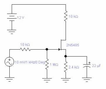
Let's start with a very simple JFET stage, the Common Source (CS) amplifier. I've picked a commonly available high-ish gain N-channel JFET for an example, the 2N5485. I picked the 2.4K source resistor for about 1/2 the available battery voltage at the drain of the JFET with a nominal 10K load resistor, and used the common 1M gate resistor. The 22uF source capacitor bypasses the source for maximum gain across range of frequencies that guitars produce. I've modeled a pickup as a voltage source with a 10K resistor in series with it - not accurate for any one pickup, but not too bad for a broad range of them.
The circuit as it sits has a gain of 17.5 - not particularly awe-inspiring, but it's constant from the low frequency roll-off of the source capacitor to pretty high in the RF spectrum. This is pretty typical of JFETs with resistor loads.
The resistor loaded JFET gain stage does have its uses. It has a very high input impedance, and can be very simply biased. It's great for on-board preamps in guitars or even inside guitar signal cord jack covers. It gives a modest boost and has a bit of soft distortion that adds some character to the sound.
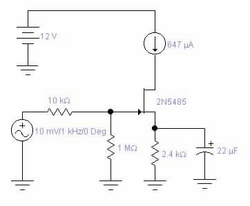 With
the addition of a constant current drain load and no other changes, we get vastly
different operation.
With
the addition of a constant current drain load and no other changes, we get vastly
different operation.
By simply trading a CCS for the 10K load resistor, the AC gain is about 175 in the audio and low RF range. In this simulation, the current source loading is ideal, and has a literally infinite impedance. The "load resistor" that the JFET's drain sees is just its own internal resistance, the equivalent drain to source resistance of the JFET itself. When we put a 1M resistor and capacitor in series to ground from the drain of the CCS loaded circuit, the gain drops to 150. This means that the internal drain resistance in this circuit is about 170K. Notice that this is now difficult to use - anything that you connect to the "output" loads the drain down too, so this particular circuit needs a high impedance buffer, like maybe a JFET source follower, to couple the signal out without loading the circuit down and losing the gain you've worked so hard to get.
It's also reasonable to use very high impedances for any inter-stage circuits that follow this one. You don't loose a lot of gain until the impedances dip under maybe 600K - if you have a perfect current source, that is.
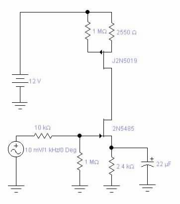
Let's see what happens when we replace the ideal CCS load with a JFET. For simplicity in understanding, we simply mirror-image the N-channel JFET with a P-channel JFET. This is perhaps the simplest of the multi-JFET stages to understand. It's clear that the bottom N-channel JFET does all the amplifying, and the upper P-channel JFET simply does anything it can on its drain to make the current through its source resistor be constant.
We could have used a bipolar transistor CCS there, but, hey, today's JFET day, and it just didn't fit the program.
Gain drops, as we would expect since there is a real JFET providing the CCS impedance, not an ideal current source. Gain is about 125 now. While this is pretty zippy gain compared to the common source JFET amplifier, it's a bit worse than the ideal CCS loaded JFET, illustrating the loading effect of anything connected to the high impedance drain.
The frequency response is nothing to write home about either. By eye, the high frequency rolloff looks to be maybe 20kHz, which is dismal indeed for a component that can otherwise easily get to UHF radio frequencies. What's going on is that the circuit is displaying its gain-bandwidth capabilility, the effect of the internal parasitic effects. Dramatically higher gain from any single device necessarily means dramatically lower bandwidth, and not only in JFETs, but all devices. Get gain, pay with bandwidth. Get bandwidth, pay with gain.
"Hey!" I hear you say, "what's that 2550 ohm resistor doing in the source circuit of the P-channel JFET? That's not a standard value."
No, it's not. Biasing two devices head to head like this is fairly tricky. Exactly matched complementary pairs would have worked with exactly matched 2400 ohm source resistors. Realistically, one of the two source resistors needs to be a trimpot if you're after max signal swing. JFETs do have much wider ranges of tolerances than bipolars do.
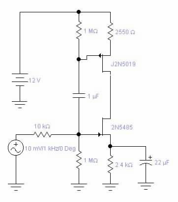
However, by adding one component to the this circuit, we get a significant change in operation. Noticing that there is no signal on the upper P-channel JFET's gate, we just connect the two gates with a capacitor. This drives both JFET inputs with the same signal, but they are phased such that an up-going signal makes the lower JFET turn on, pulling the output down, and makes the higher JFET turn off, also letting the signal go down. When the signal reverses. the top P-channel JFET pulls up, and the bottom JFET turns off, helping the output voltage go up as well.
Instead of the P-channel JFET being a simple load, it is actively helping the bottom JFET move the signal - a kind of smart load that goes the direction that will help the other device the most. In fact both devices are contributing gain, and both are acting as active loads. All of a sudden, gain is back up to about 170. This odd result happens because although both JFETs have drain resistances to load them, there are also two JFETs driving the load.
Another curious result is that the source capacitors now are unnecessary - removing the source resistor from the lower JFET or adding one to the top JFET doesn't much change the gain, and the frequency response seems to get better without them. In fact, frequency response about doubles. Frequency response is still not great by other comparisons, but it does seem to more than cover the audio band at least. The key feature that helps the gain and frequency response is that there are two devices actively creating gain and driving the combined load.
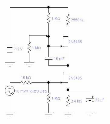
If we replace the Pchannel JFET with an N-channel, reconnect the gate-to-gate capacitor to a position between the upper gate and the lower drain, and tie the upper gate to ground with another 1M resistor, we get the JFET mu-amp circuit. It's gain is about 80 with the source capacitor in place, about 25 with the source capacitor removed. (Of course, all the gains I'm quoting here are device sensitive. There are better and worse than the 2N5485 and 2N5019.)
While the 2550 ohm source resistor is not necessary, it has no real effect on circuit operation, and I left it in for clarity about what changed - only the JFET and capacitor.
The entire trick to understanding this circuit is in noticing that the gain comes only from the bottom JFET. The upper JFET is merely acting as a source follower to pull up the output when the bottom JFET lets it rise. True, it's an odd source follower because the input is the voltage on its own source, but that is the way it works.
Connected this way, the upper N-channel JFET is still helping move the load, but is not contributing any gain itself. Also, since its input has to be driven from the drain of the lower JFET, the lower JFET is now driving the bias resistors of the top JFET, but more importantly it's also driving the JFET source impedance. This loading keeps the max gain down to about 90 even with 10M biasing resistors for the upper JFET.
In a way, you could consider that the price you pay for getting a push-pull amplifier stage that acts like a complementary push-pull stage but uses only one polarity of devices is that you lose about half the potential gain. For tube designers, with "complementary" tubes forbidden by Mother Nature, this was a very good tradeoff indeed. We at least have the choice.
So - which is best suited for what?
Obviously, the ordinary resistor loaded JFET is not well suited to really high gain jobs. However, if you run two of them stacked in series, you have a gain of 306, which is all by itself twice as large as any of the two-JFET circuits we've looked at. However, there is a potful of other components needed. Frequency response will be 'way more than needed - which may not be good, as we'll probably want some distortion and some smoothing off of the highs. And it will use up a lot of other R's and C's and board space.
The CCS loaded JFET stage, implemented with real JFETs offers a lot more gain than the resistor loaded JFET, about 125. For one additional capacitor, you get the push-pull gain stage, though, and not only is the gain is larger, you don't need source capacitors. It looks like a good trade to get rid of two large electrolytics and put in one smallish film cap, so the CCS loaded JFET stage is probably not as useful. as the push-pull true complementary stage.
Notice that both the CCS loaded JFET stage and the push-pull complementary stage are tricky to bias. Basically, you set one source resistor and twiddle the other source resistor to bring the output voltage into the linear range near the center of the power supply. They are identical as far as DC Biasing is concerned.
The "JFET mu-amp" is a push-pull stage where one JFET does all the gain and the other helps it to drive the load. This configuration has about half the gain as the push-pull complementary stage, is moderately easier to bias as only one device really contributes much to this. Interestingly, the JFET Mu-amp and the Push-pull Complementary stage have almost identical distortion profiles in their linear region. The 3rd, 4th, 5th, 6th and 7th harmonics are prominent, and the second is about half of the 3rd. I was mildly astonished that this should be so, but then I guess that they each are producing the distortion profile of a basic JFET gain stage with no feedback linearization.
The push-pull complementary stage seems to have a gain advantage while using slightly fewer parts, and you can pretty much set the asymmetry you get in distortion by setting the exact bias point. Symmetry of the onset of distortion will be set by the bias, and symmetry of distortion once it starts will be dependent on the device characteristics.
I've wondered occasionally why matching devices didn't seem to make much difference to the JFET Mu-amp. This little exercise explains that - they're not doing anything like the same job, so "matching" really doesn't apply - if the were matched, they're doing such different jobs that it wouldn't necessarily be what you want.
Just judging from the pictures on the virtual scope traces, there doesn't seem to be all that much difference in the flatness of clipping between the two push-pull stages.
What's best? I'm sure I don't know. But there are a few more choices here to play with. I gotta get some stuff breadboarded and messed with!!!