 KEY FEATURES:
DESCRIPTION:
The SAD-1024 is a general-purpose
dual 512-stage Bucket‑Brigade Device (BBD) fabricated using N-channel
silicon-gate technology to obtain flexible performance at low cost. Each
512-stage section is independent as to input, output, and clock. The
sections may be used independently, may be multiplexed to give an increased
effective sample rate, may be connected in series to give increased delay, or
may be operated in a differential mode for reduced even harmonic distortion at reduced clocking noise. Each section has its output split into two
channels so that in normal operation output is provided over each full clock
period. The SAD-1024 is packaged in a standard 16-lead dual-in-line
package. Only Vdd and GND are common to the two separate delay sections.
KEY FEATURES:
·
Two independent 512-stage delay sections.
·
Clock-controlled delay: 0.5 sec to less than
200uSec.
·
N channel silicon-gate bucket-brigade
technology.
·
Designed for self-cancellation of clocking
modulation.
·
Wide signal frequency range: 0 to more than
200kHz.
·
Wide sampling clock frequency range: 1.5kHz to more
than1.5MHz.
·
Wide dynamic range: S/N > 70db.
·
Low distortion: less than 1%.
·
Low noise: typically limited by output amplifier.
·
Single 15 volt power supply.
TYPICAL APPLICATIONS:
DEVICE CHARACTERISTICS AND
OPERATING PARAMETERS
|
PARAMETER |
Symbol |
Min |
Typ |
Max |
Units |
|
Clock Voltage (1) |
Ck1, Ck2 |
10 |
15 |
17 |
Volts |
|
Drain Supply Voltage (1) |
Vdd |
10 |
15 |
|
Volts |
|
Bias Voltage(1) |
Vbb |
|
Vdd-1 |
|
Volts |
|
Sampling Freq. |
F(Ck1, Ck2) |
0.0015 |
|
1.5 |
MHz |
|
Clock Rise-Time |
Tcr |
|
30 |
|
NSec |
|
Clock Fall Time |
Tcf |
|
50 |
|
NSec |
|
Clock Line
Capacitance |
Cc |
|
110 |
|
PF |
|
Signal Freq.
Bandwidth (-3db point) |
|
(fig 2) |
200 |
|
KHz |
|
Gain (2) |
|
|
1.2 |
|
|
|
Input Capacitance |
Cin |
|
7 |
|
Pf |
|
Input Shunt Resistance (3) |
Rin |
|
|
|
KOHm |
|
Optimum Input Bias
(4) |
|
|
16 |
|
Volts |
|
Maximum Input Signal
Amplitude |
|
1 |
2 |
|
Volts p-p |
|
Average
Temp.Coefficient of Gain (6) |
|
|
-0.01 |
|
Db/C |
|
Average
Ternp.Coefficient of Optimum Input Bias (6) |
|
|
0.8 |
|
Mv/C |
|
Absolute Maximum Voltage
(1) |
Any Pin |
0.4 |
|
+20 |
|
Notes:
CAUTION: Static discharge to any lead of this device
may cause permanent damage. Store in aluminum foil or inserted in conductive
foam. Use grounded soldering irons, tools, and personnel when handling devices.
Avoid synthetic fabrics. It Is recommended that the device be inserted into
socket before applying power.
SUMMARY OF OPERATION
The SAD-1024 is an analog sampled-data device which uses both linear and digital techniques in it's applications
and method of use. The input data is handled in analog form in discrete time,
and sampled by an external clock. Internally, the data is handled as analog
samples but moved at fixed intervals, as in a digital system. The input analog
signal is connected to the first of the 512 MOS transistors while the clock
frequency is high and is transmitted to the next section when the clock goes low
The amplitude of the input signal remains constant between sections. The clock
signals appear at the output as part of the "mix" and must be
filtered out.
DRIVE AND VOLTAGE
REQUIREMENTS
Voltage levels and limits are
given in the Device Characteristics Table. The clock inputs are two-phase
square waves. For convenience in use, Vbb may be equal to Vdd. However, for
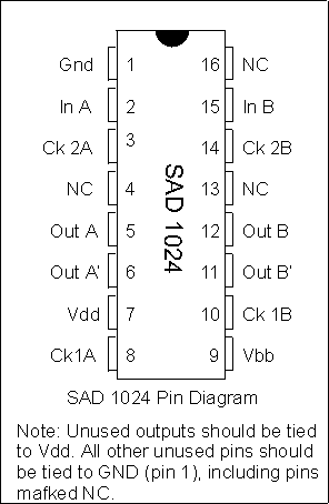
optimum performance, Vbb should be one volt less than Vdd. All unused outputs
should be connected to Vdd. All unused terminals (including the ones marked NC)
should be connected to ground. The bandwidth of the input should be limited to
less than one‑half of the clock frequency.
CLOCKING
The SAD-1024 requires
a two phase, non-overlapping clock signal. In general, the clock timing
requirement are simple enough that typical CMOS logic gates can satisfy the
non-overlapping requirements with a simple inverter chain. CMOS flip-flops such
as the CD4013 provide an excellent clock source with their Q and -Q outputs.
CIRCUIT CONFIGURATIONS
The SAD-1024 consists of two 512 element delay
sections which, except for common grounds and power input are electrically
independent. The sections may be used ill the following configurations:
1 Single-section
2. Serial
3.
Parallel-multiplex
4.
Differential
5. Multiple-devices
in series