| Guitar signal boosters have been a hot item on
guitarists' lists ever since Johnny Dallas cooked up the primordial
Dallas Rangemaster and set it loose on an unsuspecting world. While the
Rangemaster was a great advance in its day, and more than made up for
the shortcomings of the typical low-output pickup of the time,
guitarists ever since have chased boxes that could push their amps just
a little harder. For a more in-depth read on the Dallas Rangemaster, see
Rangemaster - the European Secret Weapon.
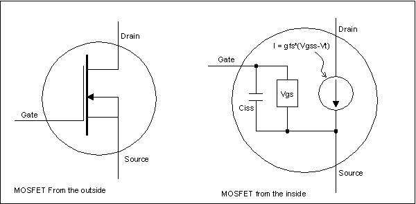
The next most venerable box in this line is the ElectroHarmonix LPB-1 (Linear Power Booster 1), Mike Matthews' single-transistor entry into the booster sweepstakes. The LPB-1 was advertised as making your amp sound louder - and perhaps it did, using up whatever headroom the amp had left and driving the bejeezus out of the input. The LPB-1 suffered from noise and the limitations of its heritage as a bipolar silicon NPN transistor gain stage. But people did like it, and bought enough to launch the ElectroHarmonix name. It was EH's first product. Somewhere along the way, the JFET was pressed into service for a single-transistor booster. This worked as well as the germanium and silicon transistors that preceeded it, but suffered from the unpredictable gain and biasing that the JFET is heir to. I'm not aware of any commercial products that resembled the single-transistor Rangemaster or the LPB-1. Recently, people have pressed the MOSFET into service in the search for the ultimate booster. There are at least a couple versions of the MOSFET booster on sale now, and more will probably join them. Let's take a look at this latest signal booster device and how it might be applied. I'll show some basic considerations, how to design it to fit YOUR needs, and some PCB layouts that you can use. Before we can design with this thing, we have to know what it does. Here's an up close and personal look under the black plastic:
From the outside, pretty simple - black plastic blob with three leads. Those leads are the gate, drain and source. The inside is a little trickier. On the right, we take an x-ray view. The source is involved in both the gate and drain circuits; in fact, it's the reference pin for this device. Everything happens with relation to the source. The gate is isolated from both the source and drain by a layer of silicon dioxide - high purity glass. The glass is 20V thick That will be important later. Even though there is no direct-current connection between the gate and source, there is a gate-to-source capacitance. "Ciss" stands for the capacitance between the gate and source and is a significant consideration we will need to worry about later. Other than that, the gate exerts a control over the current flowing from drain to source. The box marked "Vgs" is representative of a voltmeter. To figure out how much current flows between drain and source, we measure the gate-to-source voltage with that box, subtract off a bit of voltage called the threshold voltage (Vt), and then multiply the remainder by what's called the "transconductance" of the device. The transconductance (gfs) is how many amps one volt of gate-source voltage lets through. The arrow with a circle around it represents the device's transconductance. While this is the same as the electrical engineering symbol for a current source, the MOSFET current source acts more like a water valve. The transconductance doesn't really create current and force it through an external circuit, it just lets a certain amount of current through, but if and only if the external circuit can supply that much current. If the external circuit can't supply as much current as the valve wants to let through on orders from the gate-source voltage, the transconductance sucks as much as it can and as a result the voltage across the drain-source is very low. The device is said to be saturated when this happens. Resistance is denominated in units of ohms; one ohm is defined as the resistance that causes a voltage drop of one volt per ampere of current through it. Conductance and transconductance are denominated in the inverse of this, amperes per volt, which used to be called "mhos" (the reverse of ohm - get it?). However, this unit was recently (like maybe 15 years ago) renamed the "Siemen" in honor of a Mr. Siemen. You'll find the transconductance of MOSFET specified in Siemens, or more likely milliSiemens ( a thousandth of an amp per volt). Most small signal MOSFETs have transconductances in the range of 100mS to 800mS. Big power MOSFETs usually have a transconductance of about one to a few amperes per volt. To control current with a MOSFET, you just hook up a source of electricity - a 9V battery will do nicely - across the drain and source. No current flows until you also put a voltage from gate to source. When you put a gate-to-source voltage on the gate, no current flows until the gate gets to the threshold voltage of Vt; once it gets there, current starts to flow in direct proportion to the gate-source voltage.
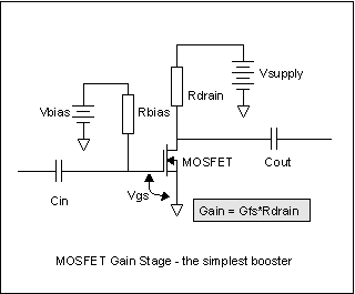
On the left is the simplest (conceptually anyway) MOSFET amplifier. We have our source of electricity in Vsupply. Since we can't tell how much current flows without measuring it, we can choose to measure it with a resistor (Rdrain) and look at the voltage across the resistor. While one ohm gives us a nice scale factor, it's a little small for most of our instruments, so lets use something easier, like 1K ohm - that is, 1000 volts per ampere, or equivalently, one volt per milliampere. That's easy for our DMM's to measure. We'll ignore Rbias, Cin and Cout for now. Cin and Cout are only useful for coupling AC signals in and out, and right now we're looking at DC gain. Rbias is in series with the gate resistance, which is maybe ten to the twelfth power ohms, so for any practical resistance we can buy, it doesn't matter. We hook up our voltmeter across Rdrain. As we vary Vbias from 0V upward, we watch the voltage on Rdrain. At first, nothing happens. There's that dead zone from zero volts up to the threshold voltage, Vt. As soon as we hit Vt, we see voltage across Rdrain, indicating that there is current flowing in it. How big is Vt? We can read it off the MOSFET manufacturer's spec sheet. For the BS170, it's 0.8V to 3.0V, with 2.1V being typical. Any two BS170's are guaranteed to be in this range. The 2N7000, another similar small signal MOSFET, is close, with a 0.8V to 3.0V range, but with a typical value of 2.0V. We'll talk more about "typical" values on datasheets later. If we have a BS170 in there, the threshold voltage will be somewhere between 0.8V and 3.0V. Let's say it's close to the typical value, an even 2.0V. When Vt goes over 2.0V, the current starts rising by gfs. For the BS170, again from the maker's datasheet, the gfs value is only shown as a "typical" of 320mS - that is, 320 milliamperes per volt. So as Vbias rises from 2.0V to 3.0V, the drain current goes from 0 ma to 320ma, right? Wrong. It would do that, except we're choking it off with our measurement method. Rdrain is 1K ohm, remember? That's 1V per milliampere. At 9ma, the entire battery voltage is dropped across the drain resistor and there isn't any more voltage to push current through the MOSFET. In fact, the current in Rdrain rises from zero milliamperes to 9ma as the Vbias rises from 2.0V to 2.028V. That additional 28 millivolts is enough to cause the MOSFET to go from completely cut off to completely saturated. (If we had used a 1 ohm measuring resistor, it would have limited the Vsupply current to 9V / 1 ohm = 9A, and we'd have seen the drain current go as high as the gate voltage told it to - until the MOSFET burned up, that is.) So we have a way to calculate the voltage gain of the MOSFET as an amplifier. In this case, the gain is the voltage swing at the drain divided by the voltage swing at the input. That's just the 9V-to-0V swing we saw at the drain, divided by the 28millivolt swing at the gate. The gain is then 9/0.028 = 321.42857. This number happens to be the gfs times the drain resistor, or 0.320S*1K. Now we get to play with Cin, Cout, and Rbias. If we put an AC signal at the outside end of Cin, that causes the Vgs voltage to swing around some. How much it swings around can be computed by figuring the amount of the signal "eaten" by the divider of Cin and Rbias. If Rbias is zero, a dead short, then Cin cannot change Vgs at all, since the gate is shorted to the Vbias battery. If Rbias is large, and Cin is large, then lots of signal can get to Vgs. How large "large" is can be computed from the voltage divider equation, substituting in the impedance of Cin (Xc=1/(2*pi*F)), or just the RC cutoff equation. The signal will essentially all get through if it's higher in frequency than F=1/(2*pi*RC). So if we make Rbias really big (doesn't matter how big, remember Rgs is ...huge...), like maybe 1Mohm, then for our guitar signals to get through, we only have to pass the lowest guitar signal of 82 Hz, and Cin can be as little as 0.0019uF and still work fine. Above the so-called cutoff frequency that we've just made 82 Hz, the impedance of Cin is much lower than Rbias, and the signal source driving Cin will see only Rbias as a load. Cin gets "transparent" above the place where its impedance is greater than Rbias's resistance. Cout will be determined by the load that the MOSFET stage has to drive, and will usually be much larger than Cin, because the loads that it drives will be much lower resistance than Rbias. Just think "bigger" there - 0.1uF to 10uF are usually good values. OK, got the AC coupling stuff in there. Now what's the AC gain? If Vbias is 0V, the gain is zero - the MOSFET is cut off, not conducting at all, so no signal appears at the drain. It now becomes obvious why we called it "Vbias" - Vbias has to be some value that turns the MOSFET on just a little so it can amplify the input signal from Cin. Thanks to our DC experimentation, we know the exact value of Vbias we need - it's the 2.0V of Vt, plus half the value that would run the MOSFET from cutoff to saturation (0.0028V) or 14 millivolts. The right value of Vbias is 2.014V. I just had an ugly thought: what if we get Vbias juuust right, then want to change to a different BS170? The new BS170 may have any Vt value from 0.8V to 3.0V. About the only certainty we have is that it will NOT have the same 2.000V Vt as our first one did.
So let's take another tack. Let's put our sensing resistor in the source lead, not the drain lead, as shown at right. For simplicity of calculation, let's use our original 2.0V Vt BS170. With Vsupply at 9V again and varying Vbias, what does a voltmeter across Rsource read? Starting at Vt = 0V, we again read 0V across Rsource until Vbias=Vt. At that point, Vgate exceeds Vsource by Vt, and the transconductance valve starts letting current through. However, unlike the resistor in the drain circuit, any current in Rsource causes a voltage across it. The voltage across it raises Vsource and therefore lessens the voltage difference between the gate and source. Rsource causes a voltage that opposes the change in Vbias - it's giving us negative feedback. We know that with only a 9V Vsupply, the voltage across Rsource can't be more than 9V even if the MOSFET becomes a dead short. Ohms law tells us the current can only be a maximum of 9ma in that case. So the voltage across Rsource can only be between 0V and 9V, and the current in it can only be between 0ma and 9ma in this circuit. Lets set Vbias to 3.0V. What's the voltage across Rsource? We have 3.0V at the gate, which is 1V higher than the 2.0V of Vt. That should cause 1V * 0.320S = 320ma of current to flow in the current valve, and therefore1K*0.32A = 320V across Rsource - which is impossible, because that would raise the source higher than the gate, and that would turn the current off again. If we remember the experiment with Rdrain, we only needed 28mv above Vt to get full current and voltage across a 1K drain resistor. So, we could guess that something less than 28mv is going to provide all the Vgs we need for a 1K source resistor. If the Vbias is 3V, Vt is 2.0V, and Vgs is 28mv, then the source resistor can't rise any higher than something like 3.0V-2.0V-0.028V = 0.972V, which means that there must be 0.972ma of current flowing, and we didn't need all 28millivolts of Vgs to get that much current. Instead, we only needed 1ma/0.32S = 0.0031mv, so the voltage on the resistor was really 3.0V-2.0V-0.0031V = 0.997V. As you can see this estimate of Vsource is a little high. Each time we do the calculation, it gets closer and closer to the real value; that's how feedback works. Depending on the exact values of the transconductance, the voltage on Rsource will settle down somewhere between 0.999 and 0.990V. We can change Vbias, and if we do, we find that the voltage on Rsource follows the changes. The voltage is always going to be Vbias minus Vt, minus whatever Vgs is needed to make that much current flow in Rsource. We know that for our "typical" BS170, the Vgs needed will be only tens of millivolts. The voltage on the source follows the voltage on the gate - we've made a source follower. The source follower is the origin of all simple biasing techniques for the MOSFET, just like the emitter follower is the origin of all simple biasing for the bipolar transistor. We can now pretty reliably design MOSFET source followers, with only this information. We just decide how much DC voltage we want across the source resistor as a fraction of the available power supply, then add to that the Vt (we can ignore the few millivolts of linear range, it's close enough). Usually that's about half the available voltage. For 9V, make the target for Rsouce about 4.5V. Then set the bias voltage at the gate of the MOSFET to 4.5V plus Vt. Vt will be 0.8V to 3.0V for the BS170, might be different for other MOSFETs. Since Vt varies, you might as well choose the "typical" value for Vt (see, I told you we'd get to that!) and you'll be really close for most examples of the type. But that's a follower, not a booster. We want a booster. Consider this: the same current flows in the drain of the MOSFET as flows in the source. It has to - the gate is a layer of glass, the current can't get out that way. There's no way to make the source terminal not follow the gate almost exactly if there is a source resistor there. But if we set the source voltage low, like maybe a volt In the circuit at left, I've done that. We now have Rsource, which sets the idle or bias current along with Vbias. We also have Rdrain, and we know the same current flows in Rdrain as in Rsource. Imagine making Rsource 1K, and the voltage across it 0.5V. Then make Rdrain 10K. Right away, we know that the voltage across Rdrain is 5V - same current as Rsource, ten times bigger resistor, has to be ten times the voltage. Georg Ohm wouldn't lie to us, would he? And we know the gain, slam dunk. It's ten. It has to be. Same current, remember? Unfortunately, there's a darker side. It's only ten. We were getting 321 out of the same MOSFET with no source resistor. Worse yet, we've said we'll use 0.5V across the source resistor - and we know that Vt can vary by as much as +1/-1.2V around the "typical" value of 2.0V. Some of the perfectly good BS170's the maker supplies won't work in the circuit as stated. Where do we go from here? Defensive Design There are two things we can do as designers. We can stick in a variable pot to adjust out the Vt variation, or we can design the circuit so it's not too terribly sensitive to the variation by making sure that most if not all of the range of Vt variation gives good results. Manufacturers **HATE** tweaking pots. It costs huge amount of money to adjust them in the manufacturing line. But we are not at the mercy of the corporate MBA's, so a tweaking pot is a possibility. But maybe we can get by without it. Here's a design procedure that will let you step through getting a MOSFET booster or buffer running.
From our earlier dinking around with the BS170, we're in good position to make some guesses. There are two main and one hybrid goal for a MOSFET transistor stage design. We either (a) want a follower or (b) want some gain. In either case, the hard thing to do is to get as linear and wide a signal range as possible. If we deliberately want to get distortion instead of linear range, we can do that to, but getting wide linear range is the hard one. Wide linear range necessarily means the widest possible voltage range at the output without bumping into either cutoff (the MOSFET drain current goes to 0, it's an open circuit), or saturation (the MOSFET looks like a short circuit, and the currents are determined only by the resistors). Let's say we want a follower. That means the source is the output. We judiciously make Rdrain be zero ohms. Ok, Ok, 50 milliohms of copper wire. We want the source to swing the widest possible range; with a 9V supply, by definition the widest possible range we could ever hope for would be a total of 4.5V up and 4.5V down, so the signal hits cutoff on negative signal peaks and saturation on positive signal peaks. That means the source has to sit at 4.5V DC, right in the middle of the power supply. It can swing 4.5V down, and 4.5V up to 9V. We know how to bias this, from our earlier experimentation. The gate needs to be Vt higher than the source. If we're using our old friend the BS170, the gate needs to be between (4.5V +0.8V) and (4.5V+3.0V) or 5.3 to 7.5V. It will "typically" be at 4.5V+2.0V, or 6.5V. We need to come up with some way to make Vbias be 5.3 to 7.5V. We could use a separate battery, as the examples have already shown, but we already have one battery, and batteries are big and expensive. Noting that the complete range of Vbias we need is less than the Vsupply battery we already have, we can just make Vbias with a resistor dividers.
Rbias1 and Rbias2 split the Vsupply to give us just the right Vbias. Since there is no, none, zip, nada current coming out of the junction of the two resistors, Ohm's law makes the calculation simple. We decide how much current we'll let flow in the two series resistors, then pick resistors that sum to Vsupply divided by that current. Rbias2 is then Vbias divided by the resistor current, and Rbias1 is what's left over. Say we decide on 1ma in Rbias1+Rbias2. Then Rbias1+Rbias2= (Vsupply/1ma), or (Rb1 + Rb1) = 9V/0.001A = 9K ohm. With Vbias=6.5V, Rb2=6.5V/0.001A = 6.5K and Rb1 = 9K-6.5K=2.5K. Ignoring for the moment that 6.5K and 2.5K are not standard values, let's see how bad it gets. Vbias is 6.5V. If Vt is really 0.8V, then Rsource sees 6.5V-0.8V = 5.3V, and a positive going signal will bang into the 9V supply when the signal is only 3.7V peak. If Vt is really 3.0V, then Rsource sees 6.5V-3V= 3.5V and the negative -going signal will bang into ground when the MOSFET cuts off on -3.5V peaks. What this is telling us is that even the worst out-in-left-field BS170 and 2N7000 devices will be OK in a source follower if we don't feed them more than 3.5V peak signals. That's not so bad. Perfect would be 4.5V, and we're mostly going to put 100mV guitar signals in there anyway. So our design is not overly sensitive to Vt, for a source follower, at least. If we want gain from the MOSFET, though, we have to choose a different arrangement of resistors and a different apportionment of the power supply voltages across the resistors and MOSFET. We already know that to get gain, the drain resistor Rdrain has to be bigger than the source resistor Rsource. Since we probably want quite a bit of gain, we probably want Rdrain to be ten or more times Rsource, which means that the DC voltage across it will be in the same proportion. So - step 1 for gain; apportion the DC voltages. Since the MOSFET can go from fully on to fully off, the output voltage of the stage can be Vsupply at its peak, and (Rsource/(Rsource+Rdrain))*Vsource at its lowest point. We'll want the biggest swing we can get, which says make Rsource small compared to Rdrain; however, remembering how much Vt varies, we need to use Rsource to help us control the variation. At a guess, let's pick the voltage across Rsource to be as big as a typical Vt. So if Vsupply is 9V, there is 2V across Rsource. Since the swing is going to be about equally divided across the MOSFET and Rdrain, let's split the remaining 7V equally between them, 3.5V each. That makes the drain voltage of the MOSFET be 5.5V. Step 2: Pick the current, which sets the resistor values. How much
current? It can be anything, but just for grins, lets try 1ma. So we
have Step 3: We need a Vbias of Vt+(Rsource*Isource) = 2.0(typically)+2.0V = 4.0V. At this point we'd calculate the biasing resistors on a real design, but I'm going to go to Step 4: We know that Vt is really going to be between 0.8V and 3.0V for the BS170 and 2N7000, so we need to check and see what the operating range really is. If Vt=3.0V really, we have generated 4.0V for Vbias and the voltage across Rsource will be the difference, or 4.0V-3.0V = 1.0V. The current through Rsource is going to be the voltage across it divided by the current through it (Ohm was right; this is really a LAW!) or 1.0V/2K = 0.5ma. The voltage across the drain resistor will be the same 0.5ma times the resistance, or (0.5ma)*(3.5K)=1.75V. The MOSFET has the rest of Vsupply across it: 9.0V-1.75V-1.0V = 6.25V. What this means is that the output voltage can't swing any higher than the 1.75V across Rdrain. We have a much smaller clean output because the Vt of the MOSFET is off at the edge of where it's supposed to be. If Vt=0.8V really, we have generated 4.0V for Vbias, and so the voltage across Rsource is really going to be Vbias (4.0v) - Vt (0.8v), or 3.2V. The current that has to flow through the resistor to get that is 3.2V/2.00K = 1.6ma. That same current will flow through Rdrain, so it will have a voltage of 3.5K*1.6ma = 5.6V across it. That means the MOSFET has only Vsupply (9v) - 5.6V - 3.2V = 0.2V across it, so the maximum negative swing the MOSFET can do is this 0.2V before it saturates. AACKKK! What happened? Only 0.2V of swing down in this case? MOSFETs have a variation in their bias voltage almost as big as JFETs, and much, much larger than bipolar transistors. Correspondingly, they are trickier to bias for large linear swings than are bipolars. MOSFETs can be biased into linear amplifiers without adjustment and tweaking, but you will either need some form of adjustment of the bias or selection of MOSFETs to get both linear (i.e. no distortion) gain and wide signal swings. So let's look at how some adjustments could be done.
Once again, we have a lot of freedom. If we like, we can just make Rbias1 and Rbias2 be zero ohms, and then Radj can be a 10K resistor. This lets us vary Vbias from 0V to +9V. However, we don't need that much range. From our earlier example, let's let Rdrain be 3.5K and Rsource be 2K. This gives us the same voltage distribution that we had for source and drain before. We want to be able to make the voltage across Rsource be 2V for Vt=0.8V to Vt=3.0V. That means Vbias needs to vary between 2.8V and 5V. If we pick a current through Rbias1, Radj, and Rbias2 of 1ma again, we can easily calculate the resistors from ohm's law. Rbias2=2.8V/0.001A = 2800 ohms. Radj=(5V-2.8V)/0.001 = 2200 ohms, and Rbias1= (9V-5V)/0.001A = 4000 ohms. Since these are not standard values, and since there is also no DC loading (the gate is an insulator), we can scale these up to convenient values. Since 50K pots are common, let's make Radj be 50K. That's an increase of 50K/2200 = 22.7 times. We can get the other resistors by multiplying by the same factor. Rbias1 = 4000*22.7 = 90909 ohms, very close to the standard 91K ohms. Rbias2 = 2800*22.7 = 63636 ohms, or about 64K; not a standard value. If we pick Rbias2 = 56K, Rbias1=82K, and Radj = 50K, we get max and min voltages of 2.68V and 5.07V - which is wide enough. We have a design that will do the full range of possible devices, even the worst ones, and it uses standard parts. The current in the biasing resistor string goes down to 9V/(82K+50K+56K) = 47uA, and is constant for any setting of Radj.
The voltage distribution on the source and drain side of the MOSFET is the same as before. The current in the bias string changes in this version, unlike variable bias network 1. We could obviously have done the same trick with Rbias1, leaving Rbias2 the same, but using Rbias1 plus an Radj to vary the bias. Even simpler perhaps, we could have put in a fixed Rbias1 and a potentiometer for Rbias2, tweaked it to the right voltage on the source, then measured the potentiometer resistance and then soldered in a fixed resistor with the resistance we measured for the potentiometer. These all work. There's yet another way. A big player we've left out of this so far is Rsource. If we set Vbias to some fixed value, then vary Rsource, the current in the drain-source side of the circuit varies. That looks like this:
The current through Rsource (and Rdrain, remember) will be Vsource/Rsource. So if Rsource is big, like a megohm, then the current in Rsource will be tiny - between 3.2v/1M and 1V/1M, or 3.2uA to 1uA. Georg Ohm to the rescue again. Across a relatively huge range of currents and values of Rsource, the voltage at the source is constant (remember our 28mv full off to full on range?), so if Rsource is 10K, the current is 3.2V/10K = 320uA to 100uA, and if Rsource is 1K, the current is 3.2V/1K= 3.2ma to 1v/1K=1ma. So very little happens at the source. But there's a whole lotta shakin' goin' on at the drain. If we had a 3.5K drain resistor like in our first examples, while Rsource varies from 1M down to 1K, the voltage across the drain resistor goes from between 3.5 and 10 millivolts to 3.5V up to ... no, it can't get to ten volts, the battery is only 9V, so the MOSFET saturates with the voltage across Rdrain at whatever voltage is not across Rsource. The drain goes from essentially the supply voltage to full saturation while the source moves only a few millivolts. There's some gain here! Collecting our thoughtsLet's take stock of what we've found out about MOSFETs.
Designing AC signal amplifiers with MOSFETsSo far, all we've done is give a nodding acknowledgement to the signals into and out of the MOSFET booster stage. Now let's look at how to use real signals. One reason for using MOSFETs is that the input impedance is so high. How high? Enormous. Effectively, the input resistance of a MOSFET is equal to the air resistance between the leads or the surface contamination of the board it's soldered into - at DC at least. With real AC signals, things get more complicated. Because the impedance of the gate is so high, it's tempting to try to design with really high input impedances. This may or may not be a good - or practical - idea. MOSFETs have a relatively high gate-source capacitance. This is the Ciss in the first picture we looked at. It acts just like a real capacitor in parallel with the gate-source inside the part. The similar capacitance exists in both bipolar transistors and in JFETs. In JFETs, it's tiny, from fractions of a picofarad to maybe a few picofarads. In MOSFETs, part of the deal with the devil the designers struck was to make a gate region with a large area to get higher current capability in the drain-to-source circuit.A signal MOSFET like the BF170 or 2N7000 may have a gate-to-source capacitance Ciss of several hundred picofarads. At low frequencies, this doesn't matter. As frequencies go up, but more importantly as the rest of the circuit impedances go up, this capacitance gets to be a real consideration.
To the AC signal, though, it does matter. The biasing resistors Rbias1 and Rbias2, with whatever portions of Radj are in series with them, load the input signal down. Power supplies are always set up to be more or less a short circuit to AC signals, so to the input signal, Rbias1 and Rbias2 look like they're in parallel, which is at least counterintuitive. The input signal then sees a resistance equal to the resistor inserted between the gate and Vbias plus the parallel combination of Rbias1 and Rbias2. If you want high input resistance, you have to have either Rbias1 and Rbias2 doubly big because they are effectively in parallel, or you have to make the inserted gate resistor big. If you pick the second way, Rbias1 and Rbias2's actual values don't matter much, only their resistor divider action in making Vbias. It's hard to find really big resistors. 10M is about all you can ordinarily find, and sometimes not that. You can make it easier on yourself by making Rgate be the really big one, and let Rbias1 and Rbias2 be normal resistor values. Then there's Ciss. If we ground the source of the MOSFET (or AC ground it by putting a big capacitor across Rsource), then Ciss just looks like a discrete capacitor of whatever value it is connected from the gate to ground. The voltage that actually reaches the gate will be determined by the impedance of the source and the value of Ciss. If Ciss is 100pF, and the source impedance is 10K (not unreasonable for a guitar pickup), you get a halving of the input signal at F = 1/(2*pi*10K*Ciss) = 159KHz. Hey! no problem! It's 'way over audio. Yes and no. Your pickups are around 10K at DC. They're inductive. Their impedance goes up with frequency, so the actual rolloff may be significantly below that. If you drive the gate with a transistor amplifier with an output impedance of 10K, you're in fat city out to low RF. There's a quirk here, though. If you don't AC ground the source, Ciss goes not to ground but to the top of the source resistor. The top of the source resistor is following the input signal around ( remember this, you'll use it one day: all source/emitter resistors are potential source/emitter follower outputs). If the "follow" was perfect, there would be no voltage change across Ciss and so Ciss couldn't affect the Vgs. It would be as if it wasn't there. In the real world, the signal at Rsource is not exactly as big as the input signal, so there is some signal voltage across Ciss, but much smaller than the full signal. If the gain from gate to source is 0.995 (not unreasonable), then Ciss has an effect as though it was only 5/1000 as big as it really is. Source followers can have really high input impedances and really high frequency responses. This is a consequence of what seems to be a natural law - you want more gain, you have to pay for it in more devices or narrower frequency response. But lets forge ahead on the amplifier front. Let's make a useful amplifier. Let's pick some voltages, bias an amplifier and see what can be done with it. Gotta start with objectives; shoot for biggest undistorted signal swing, and highest gain. Since we're stompbox guys, we'll use a 9V battery. We already know that the biggest undistorted signal swing will be when Vsource is 0V and the power supply voltage is divided evenly by the voltage across the MOSFET and the drain resistor. This is also where variations in Vt matter most. One option is to make Rsource = 0, Vbias minimum = 0.8V, Vbias max = 3.0V and Rdrain whatever you decide for current and gain. The gain will be gfs *Rdrain. Gfs is fixed per device, Rdrain goes up as bias current goes down, so you get higher current and lower gain together. Going for low current gets you high gain, but lower currents sometimes introduce a grainy noisy texture to the sound, because current flow is quantized into electrons and at very low currents you can actually hear this as a faint "rain on the roof" noise. Tubes do the same thing. Since there is no Vsource to help buffer out Vt differences from device to device, every single MOSFET amplifier will likely need its bias tweaked. This is not a problem for DIY'ers, but it's a massive problem for manufacturers. Another is for Vmosfet to be about 4V, Vrdrain = 4V, Vrsource = 1V. This helps some with the Vt variation, but you're still going to need tweaking for most cases, and the gain can only be 4 (Current in drain and source is the same, so the voltages across Rdrain and Rsource is in proportion to their resistance, and gain = Rdrain/Rsource). There's been a massive loss of gain. We can get it back by using a source capacitor. This is a big-value capacitor that parallels the source resistor. The source is held at some voltage for DC biasing conditions, but is held at AC ground for signals. The source capacitor makes the gain be gfs* Rdrain again for all frequencies where the capacitor's impedance is much smaller than the source resistor. We have the gain back, and potentially a more stable and less tweaking-prone design.
... to be continued... It's coming. Gotta finish writing the theory first.
|
 This sounds like it
could be an amplifier - and it is. So let's make an amplifier.
This sounds like it
could be an amplifier - and it is. So let's make an amplifier. 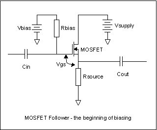 AACK!!
So any new BS170 we put in will most likely make our amplifier NOT work!
That's right. Our amplifier is highly device sensitive. We have to
figure out how to make it less sensitive to the device or we'll never be
able to make any MOSFET amplifiers without tweaking Vbias around for
each one.
AACK!!
So any new BS170 we put in will most likely make our amplifier NOT work!
That's right. Our amplifier is highly device sensitive. We have to
figure out how to make it less sensitive to the device or we'll never be
able to make any MOSFET amplifiers without tweaking Vbias around for
each one.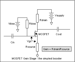 ,
and stick another resistor into the drain circuit, a bigger resistor,
then with the same current flowing in the bigger resistor, the signal
part of the current will be bigger, and we'll have gain. It's that
simple.
,
and stick another resistor into the drain circuit, a bigger resistor,
then with the same current flowing in the bigger resistor, the signal
part of the current will be bigger, and we'll have gain. It's that
simple.  Like this...
 In the circuit at
right, we do the obvious thing - we stick in a third resistor, but a
resistor that can be tapped at various points on the resistor. The
potentiometer Radj is inserted between Rbias1 and Rbias2. What are the
values?
In the circuit at
right, we do the obvious thing - we stick in a third resistor, but a
resistor that can be tapped at various points on the resistor. The
potentiometer Radj is inserted between Rbias1 and Rbias2. What are the
values?  Here's another way. We
can make Radj a variable resistor on one side of the tap for the gate
bias. When Radj=0, the gate bias is just (9V*Rbias2)/(Rbias1+Rbias2). So
to set this one up, we calculate Rbias1 and Rbias2 for the minimum
necessary bias voltage of 2.8V, and then a second version where Rbias1
is the same value as we just calculated, but Rbias2 is now bigger, and
the bias voltage is 5V. The difference in the two Rbias2 values is the
value for Radj, and the final Rbias2 value is the smaller one we
calculated first.
Here's another way. We
can make Radj a variable resistor on one side of the tap for the gate
bias. When Radj=0, the gate bias is just (9V*Rbias2)/(Rbias1+Rbias2). So
to set this one up, we calculate Rbias1 and Rbias2 for the minimum
necessary bias voltage of 2.8V, and then a second version where Rbias1
is the same value as we just calculated, but Rbias2 is now bigger, and
the bias voltage is 5V. The difference in the two Rbias2 values is the
value for Radj, and the final Rbias2 value is the smaller one we
calculated first.  We can just pick a
good, middle of the road Vbias and twiddle Rsource. If, for instance, we
set Vbias to 4V with fixed values for Rbias1 and Rbias2, and we then
vary Rsource, what happens? We already know that within the limits of
burning things up, the voltage at the source terminal will be Vbias
minus Vt. So in all (reasonable) cases, Vsource will be between
4.0V-0.8V and 4.0V-3.0V, or 3.2 to 1V.
We can just pick a
good, middle of the road Vbias and twiddle Rsource. If, for instance, we
set Vbias to 4V with fixed values for Rbias1 and Rbias2, and we then
vary Rsource, what happens? We already know that within the limits of
burning things up, the voltage at the source terminal will be Vbias
minus Vt. So in all (reasonable) cases, Vsource will be between
4.0V-0.8V and 4.0V-3.0V, or 3.2 to 1V. 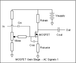 Here's a somewhat
typical MOSFET stage. I've added a series resistor between the gate of
the MOSFET and the adjustable bias voltage. This resistor could just be
a wire - a resistor of a few milliohms - or it could be high, many
megohms and make no difference at all to the MOSFET or its bias because
the gate is an open circuit. No bias current flows.
Here's a somewhat
typical MOSFET stage. I've added a series resistor between the gate of
the MOSFET and the adjustable bias voltage. This resistor could just be
a wire - a resistor of a few milliohms - or it could be high, many
megohms and make no difference at all to the MOSFET or its bias because
the gate is an open circuit. No bias current flows.