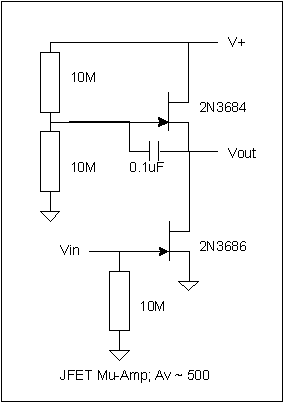
 As originally
used, the mu-amp/minibooster was two N-channel JFETs stacked from a positive
power supply to ground. The bottom JFET was biased by a gate resistor to ground,
and the top JFET was biased by two 10M resistors to half the power supply.
As originally
used, the mu-amp/minibooster was two N-channel JFETs stacked from a positive
power supply to ground. The bottom JFET was biased by a gate resistor to ground,
and the top JFET was biased by two 10M resistors to half the power supply. Copyright R.G. Keen 2001. All rights reserved. No permission for local copies or redisplay from web sites other than http://www.geofex.com.
A short history of the mu-amp in effects
The mu-amp is a very old circuit. It was reasonably common during the vacuum tube era, where it offered the opportunity to get a lot of gain and signal output out of common, garden variety triodes. Later, National Semiconductor published a JFET adaptation of the mu-amp in their JFET applications notes in a collection of JFET cookbook circuits. Later, effects experimenter Jack Orman used the mu-amp for a guitar gain circuit, renaming the circuit the "minibooster". The use of the mu-amp has been adapted into several DIY effects circuits from there. You can see the original circuit on National Semi's web page at http://www.national.com/an/AN/AN-32.pdf .
National's JFET Mu-amp
As originally
used, the mu-amp/minibooster was two N-channel JFETs stacked from a positive
power supply to ground. The bottom JFET was biased by a gate resistor to ground,
and the top JFET was biased by two 10M resistors to half the power supply.
With the bottom JFET having Vgs=0, it was biased at Id=Idss. The top JFET was then forced to conduct the same current by the lower JFET pulling down on its source lead. The voltage that the top source/lower drain settled at was whatever Vgs for the top JFET that made the current work. In practice, this was somewhat above the V+/2 voltage on the gate of the upper JFET.
What happens with signal? If a small upward voltage is connected to the gate of the lower JFET, it turns the lower JFET on a bit, and the lower drain sucks in more current. The current can't come from the capacitor, as the capacitor is effectively in series with a 5M resistor. It can only come out of the source of the upper JFET. The source voltage then drops, and so the capacitor pulls the gate of the upper JFET down as well. This has the effect of turning the upper JFET off more, which lets the voltage on the source drop further. In effect, the upper JFET is actively contributing to the voltage swing on the lower JFET's drain. The reverse happens when there is a negative-going signal on Vin.
The easiest way to think of this is that the two devices are in push-pull for voltage gain. When the lower JFET's drain starts down, the upper JFET turns off a bit to help the lower JFET's drain fall. When the lower JFET's drain rises, the upper JFET's source rises to help it. Neat trick!
The gain available in this setup is large, about equal to the lower JFET's mu divided by two. Gains of 400 to 600 are common, depending on device.
But it's not perfect...
 There is a
problem there, though. We very seldom want voltage gain for its own sake.
Remember that the assumption was that the loading on the drain of the lower JFET
was only the upper JFET source and the 5M of the biasing network through the
capacitor. What's connected to Vout?
There is a
problem there, though. We very seldom want voltage gain for its own sake.
Remember that the assumption was that the loading on the drain of the lower JFET
was only the upper JFET source and the 5M of the biasing network through the
capacitor. What's connected to Vout?
If anything much less than 1M is connected to Vout, voltage gain starts falling. It falls so fast that something 500K or more has to be considered the lower limit of loading for the circuit. Otherwise, you're giving up the gain you were clever enough to get in the first place.
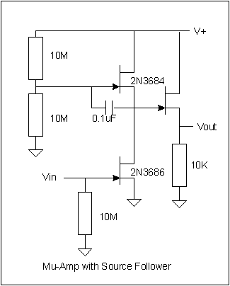
One way around this is to buffer the output with a source follower. A third JFET does this easily, as shown at left. The loading on the mu-amp is not taxing at all, and none of the bad effects of loading occur.
But you have to buy that third JFET.
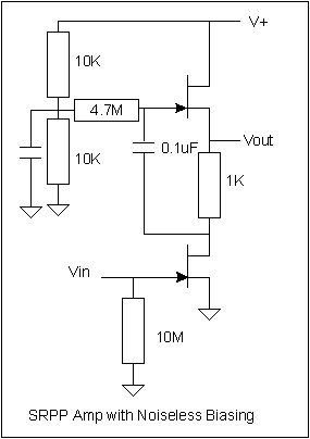
There's another problem lurking in all of these circuits. Those two 10M resistors that are biasing the upper JFET also make noise. They have a significant voltage across them, and that means that their thermal noise and any voltage-gradient noise will shine through.
Some fixes!
 We can make some
simple changes that will help.
We can make some
simple changes that will help.
Low noise biasing is the easiest to do. Just change those 10M's to 10K, and hook a 4.7M or 5.1M resistor to the gate of the upper JFET. This simple change reduces the voltage gradient across the high (1/2M) biasing resistor, feeds it from a low impedance (5K, the two 10K's in parallel) source to reduce its thermal noise, and offers the ability to shunt thermal noise from the junction of the two 10K's to ground.
This trick is known as "noiseless biasing". Note that if you have several JFET stacks as some effects pedals do, you can run a single 1/2 meg resistor to each one from the same two 10K resistors and they'll be perfectly happy. You can do this on any mu-amp setup.
The 1K resistor between the source of the upper JFET and the drain of the lower JFET works some magic. The upper JFET is perfectly capable of being a source follower with an output impedance of maybe 200 ohms. However, it can't do that and keep the drain of the lower JFET happy at the same time. Putting a 1K resistor in series lets it do both. The 1K resistor isolates the upper source from the lower drain so that the upper source can drive loads down to about 10K ohms with only trivial loss of gain. It doesn't change the voltage/current the lower drain sees by much.
However, the insertion of the 1K resistor does kick the gain up! I set up a prototype with a switch across the 1K so I could switch between the two circuits. With the 1K in, you get about twice the gain, in addition to lower output impedance.
A fair number of mu-amp circuits in the DIY effects community add a source emitter between the lower JFET's source and ground. That works the same way in the SRPP. What it does is increase the negative Vgs bias on the lower JFET to some higher value, causing the static current in the two JFETs to become lower than Idss for the pair. Any gain lost to the source resistor can be made back up by bypassing it with a suitably sized capacitor.
So if you're into tinkering with mu-amps, try an SRPP. Frankly, that's a horrible name. Maybe we should call it the macro-booster - what do you think?