Bypassing and Switching with the CD4053 CMOS Analog MUX
Copyright 2000 R.G. Keen. All rights reserved. No permission
for local copies or serving from web pages other than http://www.geofex.com.
I get a lot of questions on how to do an electronic bypass that approaches
the performance of a true bypass mechanical switch. This has been hard in the
past due to limitations of the switching elements available and a lack of
understanding of how to use them. Here's an electronic switch that approaches
the performance of mechanical true bypass switches. It's cheap and easy. Try it!
 The basis for the switch is
the CD4053 analog multiplexer IC. This is a CMOS logic chip that contains three
SPDT CMOS analog switches and the attending control logic to make them work.
People who have tried these before have often complained that they pop or
distort, and have then moved on and forgotten them.
The basis for the switch is
the CD4053 analog multiplexer IC. This is a CMOS logic chip that contains three
SPDT CMOS analog switches and the attending control logic to make them work.
People who have tried these before have often complained that they pop or
distort, and have then moved on and forgotten them.
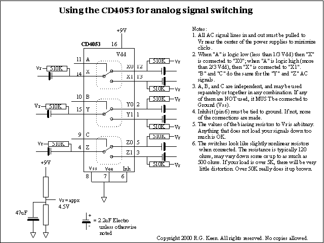
There are some tricks to using this chip. First - the analog inputs and
outputs need to be held somewhere near the middle of their power supply. The
4053 does have a "Vee" supply pin that lets it control signals near
0V, but that is often a fair amount of trouble to use. the simplest thing to do
is to AC couple the in/out pins and bias them to the middle of the 4053's power
supply. In a +9V system, this only needs a two resistor divider and a cap, then
a resistor and capacitor per in/out pin.
Yes, this is a pain, eats up board space, and is complicated. It works,
though. When biased this way, the CD4053 has little or no distortion and no
perceptible switching pops - exactly what we want.
The three SPDT switches are independent. As noted in the illustration, when
"A" (pin 11) is low, "X" (pin 14) is connected to
"X0" (pin 12). When "A" is high, "X" is connected
to "X1" (pin 13). "B" and "C" do the same
switching control for "Y" and "Z". "Low" means
below 1/3 of the Vdd voltage, or 3V in a 9V battery system. "High" is
over 6V. Like all CMOS, it's important to NEVER leave an input pin unterminated,
so all control pins that are not being used must be tied to ground or some
definite logic level.
When a switch is connected, it looks like a moderately nonlinear resistor
between pins. The resistance varies with the signal voltage from pin to pin,
which really means that for low distortion, you have to keep the current through
the switch low. The switch looks like a 120 to 500 ohm resistor. So if it's
switching things that are themselves 10's of K ohms or higher, the distortion
will be low.
So - let's make a bypass switch.
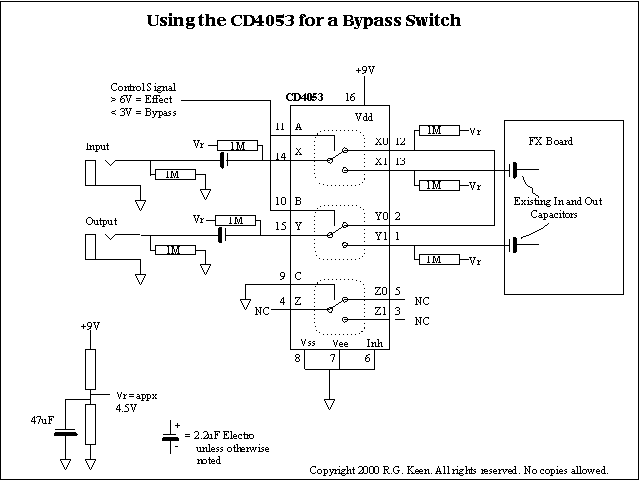 In the illustration at
right, I've shown the basic hookup for a bypass switch. We don't need one of the
three SPDT's, so I've tied "C" to ground and left the switching pins
open. The other two are hooked up in the old standard "true" bypass
fashion. Notice that it would actually be better to use one of the alternate
true bypass setups to avoid the signal passing through two of the switches when
bypassed, but this hookup does work OK in most cases.
In the illustration at
right, I've shown the basic hookup for a bypass switch. We don't need one of the
three SPDT's, so I've tied "C" to ground and left the switching pins
open. The other two are hooked up in the old standard "true" bypass
fashion. Notice that it would actually be better to use one of the alternate
true bypass setups to avoid the signal passing through two of the switches when
bypassed, but this hookup does work OK in most cases.
The in/out pins are all biased to half the 9V supply; notice that the
"bypass" path from pin 12 to pin 2 is only biased once, and needs no
capacitor, so we save some parts there over the general case.
The input/output capacitors of the effect can also be presumed to be adequate
to keep the bias DC value out of the effect, so we save two more caps there.
All we need now is a control signal. I've hooked the A and B controls
together. When both are driven high, the effect is heard. When both are low, the
effect is bypassed. Notice that if we had other uses for the third switch in the
CD4053, we could use that as well, for either AC or DC switching.
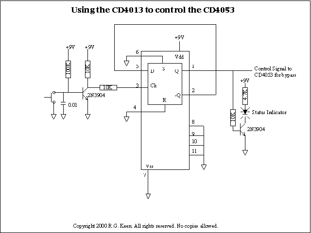 A simple and easy way to
control a CMOS logic chip is with another one. The CD4013 is a very cheap,
highly available dual D flipflop. We can use one section of it to control the
4053. It's guaranteed by design to drive the two logic inputs properly.
A simple and easy way to
control a CMOS logic chip is with another one. The CD4013 is a very cheap,
highly available dual D flipflop. We can use one section of it to control the
4053. It's guaranteed by design to drive the two logic inputs properly.
We use a momentary switch to ground the base of an ordinary transistor. This
turns the transistor off, and a capacitor on the base of the transistor prevents
any switch bounce from tripping the flipflop more than once. The transistor's
collector goes high cleanly, clocking the flipflop. The D input to the flipflop
is connected to the "-Q" output, which is the opposite of the logic
state the flop was clocked to the last time. Hooking it up this way means that
every clock pulse it will switch to the opposite state from where it is sitting
now.
From there, we just connect the "Q" output to the A and B control
lines, and the bypassing works. We'd like to have an indicator of the status, so
we add a transistor to buffer the Q output so when it's high, an LED is lit.
But there are also many ways to do this.
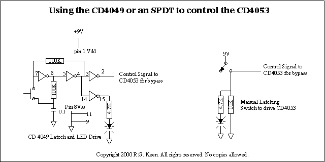 Here are two more. On the
left, I've used a CD4049 hex inverter IC to make a toggling flipflop and an LED
driver. The two inverters on the left form a latch. When the power is turned on,
one of them will come up a little bit before the other one, and so its output
will driver the input of the other inverter high, which drives its output low,
which reinforces the higher inverter's output at being high. The thing is
guaranteed to lock up with either pin 6 or pin 4 fully logic high, and the other
one low.
Here are two more. On the
left, I've used a CD4049 hex inverter IC to make a toggling flipflop and an LED
driver. The two inverters on the left form a latch. When the power is turned on,
one of them will come up a little bit before the other one, and so its output
will driver the input of the other inverter high, which drives its output low,
which reinforces the higher inverter's output at being high. The thing is
guaranteed to lock up with either pin 6 or pin 4 fully logic high, and the other
one low.
If we guess that pin 6 comes up high, pin 4 will be low. The 0.1uF capacitor
charges to +9V through the 100K capacitor. It's perfectly happy to stay this way
forever. However, if we press the momentary switch that connects the capacitor
to pin 7, the +9V on the capacitor pulls pin 7 high. The 100K resistor from pin
4 to pin 7 prevents the logic low output at pin 4 from fighting off the
capacitor, so pin 7 goes high. That forces pins 5 and 6 low, which makes pin 4
high, and now pin 4 is holding pin 7 high also. All this happens in the first
100nSec or so when the switch is pressed. Switch bounce can only reinforce the
action. Both inverters change state, and hold each other in the new condition.
The switch opens before the capacitor can change voltage much, and the capacitor
begins charging to 0V through the 100K resistor. The flip has flopped.
We have four more inverters, might as well use them. There is no reason to
choose the high or low state of pin 4 for effect on or off, so we can just
attach two of the four remaining inverter inputs to pin 4; these are pin 3 and
pin 14. Pin 2 then drives the A and B control signal, and pin 15 drives a higher
current LED.
And manual non-momentary switches also work. The circuit on the right shows
how to provide the control signal and drive an LED with a single switch.